PathWave Electrical Performance Scan (EP-Scan) is an advanced software tool from Keysight Technologies for predictive and post-layout electrical analysis of printed circuit boards (PCBs). It integrates with EDA layout tools to extract electrical models, perform rapid 3D electromagnetic (3DEM) simulation on critical nets, and provide pass/fail validation against user-defined electrical performance rules—all before physical prototyping. This “shift-left” approach identifies potential signal degradation, crosstalk, and power delivery issues early in the design cycle, saving significant time and cost.
PathWave EP-Scan is developed for high-speed digital design engineers, RF/microwave engineers, signal integrity (SI) and power integrity (PI) analysts, and PCB validation specialists. It is specifically designed for professionals working on cutting-edge electronics where signal performance at multi-gigabit data rates (SerDes, DDR, PCIe) or high-frequency analog/RF behavior is critical.
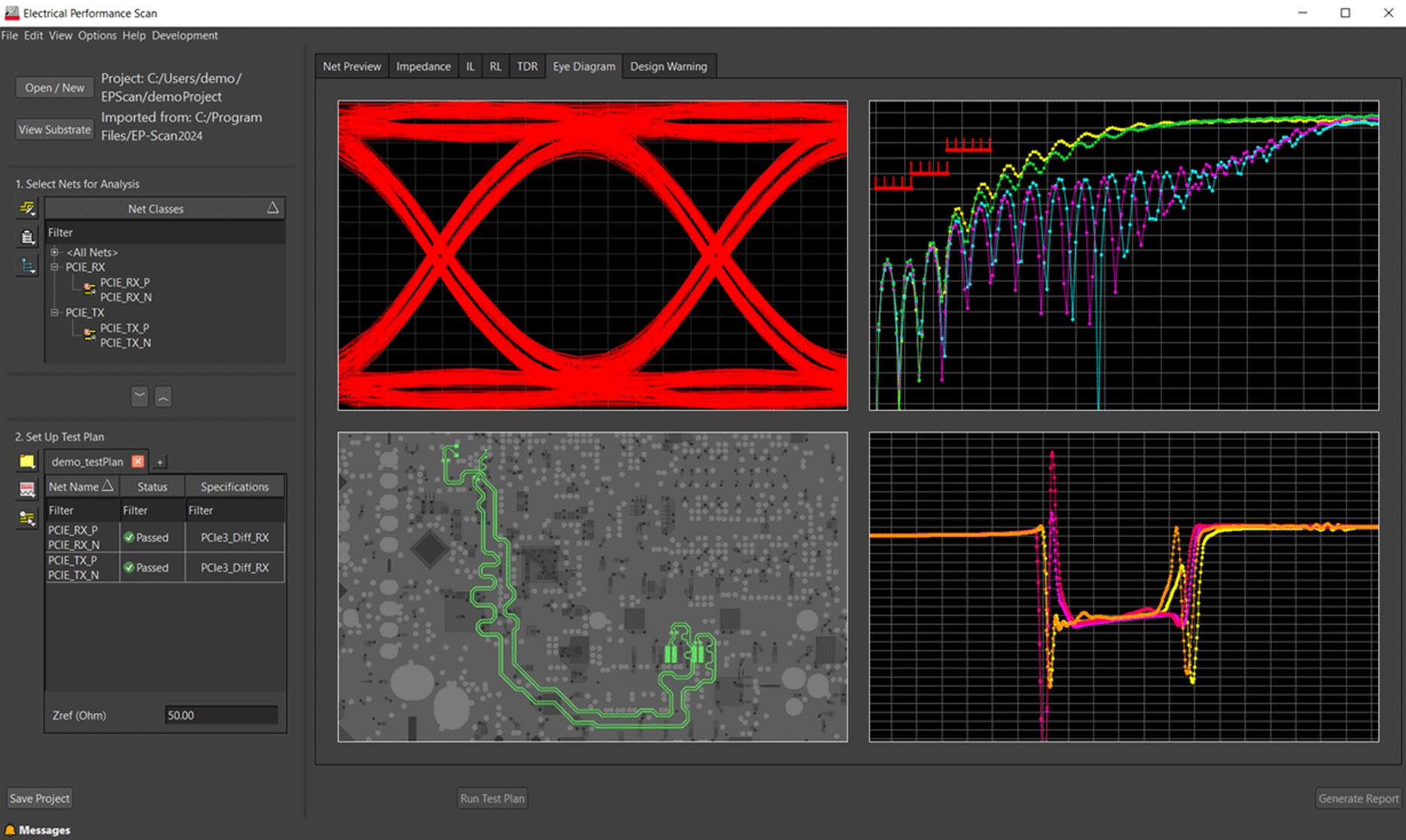
Automated Design Rule Checking (DRC) for Electrical Performance: Goes beyond geometric DRC to validate electrical behavior against SI/PI metrics (impedance, insertion loss, crosstalk, return loss, power plane resonance).
Integrated 3D Electromagnetic (3DEM) Solver: Performs accurate S-parameter extraction for critical channels (vias, connectors, complex interconnects) using a built-in, fast 3D field solver.
Pre-Layout & Post-Layout Analysis: Works in the schematic phase for predictive analysis and with finished PCB layouts (importing ODB++, IPC-2581, or native EDA formats) for final validation.
Channel Simulation & Compliance Testing: Simulates entire high-speed channels (from transmitter to receiver) and checks compliance with industry standards (PCIe, USB, DDR, Ethernet).
Power Integrity Analysis: Identifies power delivery network (PDN) issues like excessive impedance, plane resonance, and decoupling capacitor effectiveness.
Batch Mode & Dashboard Reporting: Automates the analysis of hundreds or thousands of nets and generates comprehensive, visual pass/fail reports highlighting violations by severity.
Seamless EDA Integration: Direct integration with major PCB design environments (Cadence Allegro, Siemens Xpedition, Mentor PADS) for a cohesive workflow.
The 2024 release emphasizes AI-driven insights, expanded standard coverage, and cloud-enabled scalability:
AI-Assisted Violation Root-Cause Analysis: New machine learning algorithms suggest the most likely physical causes (e.g., specific via field, coupling length) for identified electrical rule violations, speeding up debugging.
Expanded Standard Libraries: Updated and extended compliance kits for the latest versions of high-speed standards (PCIe 6.0, DDR5, USB4, etc.).
Cloud-Native Simulation Options: Ability to offload large 3DEM simulation jobs to scalable cloud compute resources (Keysight PathWave Cloud) for faster turnaround on complex designs.
Enhanced Visualization & Debugging: Improved 3D visualization of electromagnetic fields and current distributions on violations, providing intuitive insight into problem areas.
Performance & Capacity Improvements: Optimized solver performance for larger, more complex PCB designs with higher layer counts and denser components.
OS: Windows 10/11 Pro or Enterprise (64-bit), version 21H2 or later
CPU: High-performance multi-core processor (Intel Xeon or Core i9 / AMD Ryzen Threadripper or Ryzen 9 recommended)
RAM: 32 GB minimum (64 GB or more highly recommended for large designs and 3DEM simulation)
GPU: Professional-grade graphics card with latest drivers and 8 GB+ VRAM (NVIDIA RTX A-series or Quadro series)
Disk Space: 40 GB free space for installation (NVMe SSD strongly recommended for performance)
Other: Latest graphics drivers; Internet connection for license management and cloud features.
Price: 125 $
Price Currency: $
Operating System: Windows
Application Category: Electronics


Reviews
There are no reviews yet.