Z-Planner Enterprise is a specialized, field-solver-based software for precise PCB stackup planning and materials selection. It moves beyond rule-of-thumb calculations by using an integrated electromagnetic field solver to accurately model loss, impedance, and crosstalk in multilayer board designs. The software provides complete control over the entire stackup design and fabrication process, featuring a comprehensive library of dielectric materials with real-world dispersion and loss data. By enabling accurate modeling of the stackup as it will be physically built, Z-Planner eliminates costly guesswork, prevents post-fabrication surprises, and ensures first-pass success in high-speed PCB fabrication. It serves as a critical bridge between design intent and manufacturing reality.
This precision engineering software is designed for:
Signal Integrity (SI) & Power Integrity (PI) Engineers designing high-speed digital and RF boards.
PCB Design Leads & Architects responsible for defining board layer stackups and materials.
RF/Microwave Engineers designing controlled impedance structures and transmission lines.
PCB Fabrication Engineers who need to translate design intent into manufacturable specifications.
Component & Materials Engineers selecting dielectrics and laminates for optimal performance.
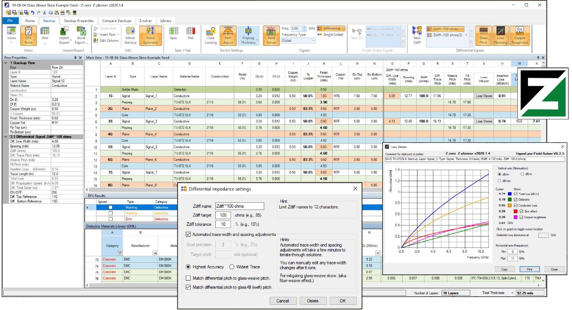
Integrated 2.5D Field Solver: Performs accurate electromagnetic simulations to calculate impedance, propagation delay, insertion loss (IL), and crosstalk for complex stackups.
Comprehensive Materials Library: Includes an extensive database of laminates, prepregs, and films from major manufacturers (Isola, Rogers, Panasonic, etc.) with frequency-dependent Dk/Df data.
Loss Planning Environment: Models conductor roughness (Huray, Hammerstad models) and dielectric losses to predict total channel performance up to mmWave frequencies.
Seamless EDA Integration: Directly interfaces with popular Signal Integrity tools (Keysight ADS, Cadence PowerSI, SIwave) and exports stackup definitions for PCB layout tools (Allegro, Xpedition, Altium).
Fabrication-Ready Documentation: Generates detailed stackup drawings, impedance tables, and material specification sheets for clear communication with PCB fabricators.
“What-If” Scenario Analysis: Allows rapid comparison of different material sets, layer counts, and target impedances to optimize cost, performance, and manufacturability.
Enhanced Multi-Gigabit Channel Modeling: New models for accurately predicting performance for PCIe Gen6/7, DDR5, and 224G Ethernet applications.
Advanced Copper Roughness Modeling: Updated surface treatment models for Ultra Low-Profile (ULP) and Very Low-Profile (VLP) copper foils.
Extended Materials Database: Dozens of new materials added, including ultra-low-loss dielectrics for high-frequency automotive radar and 5G applications.
Improved Fabricator Collaboration Portal: Streamlined workflow for sharing and commenting on stackup proposals directly with manufacturing partners.
Automated DFM (Design for Manufacturability) Check: New rulesets to flag potential fabrication issues related to material availability and processing constraints early in the design cycle.
OS: Windows 10/11 Pro (64-bit)
RAM: 8 GB minimum (32 GB recommended)
CPU: Intel Core i7/i9 or AMD Ryzen 7/9 (High single-thread performance preferred)
Storage: 4 GB free space (SSD recommended)
Price: 325 $
Price Currency: $
Operating System: Windows
Application Category: Electronics


Reviews
There are no reviews yet.